- 您现在的位置:买卖IC网 > Sheet目录493 > NVD5863NLT4G (ON Semiconductor)MOSFET N-CH 60V 14.9A DPAK-4
�� �
�
�NVD5863NL�
�Power� MOSFET�
�60� V,� 7.1� m� W� ,� 82� A,� Single� N� ?� Channel�
�Features�
�?� Low� R� DS(on)� to� Minimize� Conduction� Losses�
�?� High� Current� Capability�
�?� Avalanche� Energy� Specified�
�?� AEC� ?� Q101� Qualified�
�?� These� Devices� are� Pb� ?� Free,� Halogen� Free/BFR� Free� and� are� RoHS�
�Compliant�
�MAXIMUM� RATINGS� (T� J� =� 25� °� C� unless� otherwise� noted)�
�V� (BR)DSS�
�60� V�
�http://onsemi.com�
�R� DS(on)�
�7.1� m� W� @� 10� V�
�9.0� m� W� @� 4.5� V�
�I� D�
�82� A�
�Parameter�
�Symbol�
�Value�
�Unit�
�Drain� ?� to� ?� Source� Voltage�
�Gate� ?� to� ?� Source� Voltage�
�V� DSS�
�V� GS�
�60�
�"� 20�
�V�
�V�
�D�
�Continuous� Drain� Cur-�
�rent� R� q� JC� (Note� 1)�
�Power� Dissipation� R� q� JC�
�(Note� 1)�
�Steady�
�State�
�T� C� =� 25� °� C�
�T� C� =� 100� °� C�
�T� C� =� 25� °� C�
�T� C� =� 100� °� C�
�I� D�
�P� D�
�82�
�58�
�96�
�48�
�A�
�W�
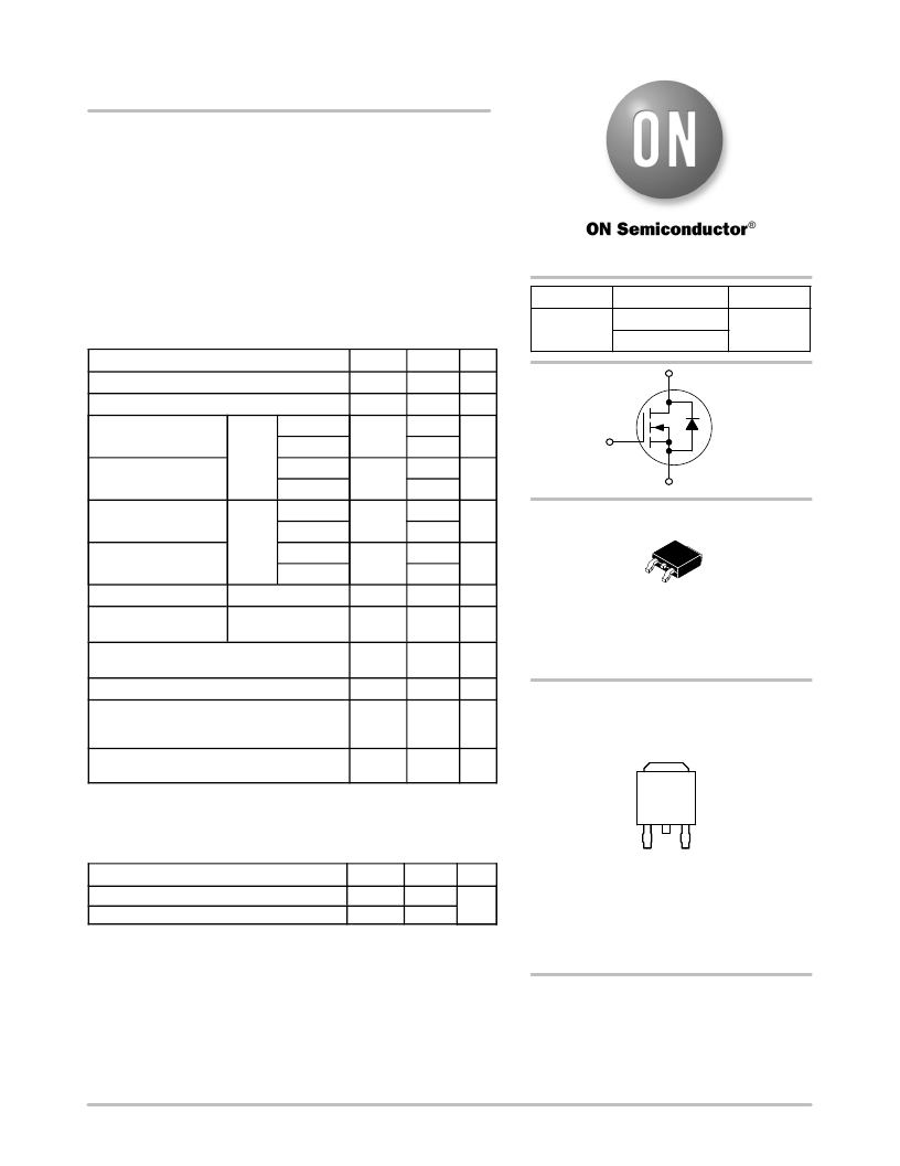
�G�
�S�
�N� ?� Channel�
�T� A� =� 25� °� C�
�Continuous� Drain� Cur-�
�rent� R� q� JA� (Notes� 1� &� 2)�
�Power� Dissipation� R� q� JA�
�(Notes� 1� &� 2)�
�Pulsed� Drain� Current�
�T� A� =� 25� °� C�
�Steady� T� A� =� 100� °� C�
�State�
�T� A� =� 100� °� C�
�T� A� =� 25� °� C,� t� p� =� 10� m� s�
�I� D�
�P� D�
�I� DM�
�14.9�
�11.5�
�3.1�
�1.6�
�500�
�A�
�W�
�A�
�1� 2�
�3�
�4�
�Current� Limited� by�
�Package� (Note� 3)�
�T� A� =� 25� °� C�
�I� Dmaxpkg�
�60�
�A�
�DPAK�
�CASE� 369AA�
�Operating� Junction� and� Storage� Temperature�
�Source� Current� (Body� Diode)�
�Single� Pulse� Drain� ?� to� ?� Source� Avalanche�
�Energy� (T� J� =� 25� °� C,� V� DD� =� 50� V,� V� GS� =� 10� V,�
�I� L(pk)� =� 23� A,� L� =� 1.0� mH,� R� G� =� 25� W� )�
�Lead� Temperature� for� Soldering� Purposes�
�(1/8� ″� from� case� for� 10� s)�
�T� J� ,� T� stg�
�I� S�
�E� AS�
�T� L�
�?� 55� to�
�175�
�82�
�265�
�260�
�°� C�
�A�
�mJ�
�°� C�
�STYLE� 2�
�MARKING� DIAGRAMS�
�&� PIN� ASSIGNMENT�
�4�
�Drain�
�Stresses� exceeding� Maximum� Ratings� may� damage� the� device.� Maximum�
�Ratings� are� stress� ratings� only.� Functional� operation� above� the� Recommended�
�Operating� Conditions� is� not� implied.� Extended� exposure� to� stresses� above� the�
�Recommended� Operating� Conditions� may� affect� device� reliability.�
�THERMAL� RESISTANCE� MAXIMUM� RATINGS�
�Parameter� Symbol� Value� Unit�
�2�
�1� Drain� 3�
�Gate� Source�
�Junction� ?� to� ?� Case� ?� Steady� State� (Drain)�
�R� q� JC�
�1.6�
�°� C/W�
�Y�
�=� Year�
�Junction� ?� to� ?� Ambient� ?� Steady� State� (Note� 2)� R� q� JA� 48�
�1.� The� entire� application� environment� impacts� the� thermal� resistance� values�
�shown,� they� are� not� constants� and� are� only� valid� for� the� particular� conditions�
�noted.�
�2.� Surface� ?� mounted� on� FR4� board� using� a� 650� mm� 2� ,� 2� oz.� Cu� pad.�
�3.� Continuous� DC� current� rating.� Maximum� current� for� pulses� as� long� as� 1�
�second� are� higher� but� are� dependent� on� pulse� duration� and� duty� cycle.�
�WW� =� Work� Week�
�5863L� =� Device� Code�
�G� =� Pb� ?� Free� Package�
�ORDERING� INFORMATION�
�See� detailed� ordering� and� shipping� information� in� the� package�
�dimensions� section� on� page� 5� of� this� data� sheet.�
�?� Semiconductor� Components� Industries,� LLC,� 2011�
�December,� 2011� ?� Rev.� 1�
�1�
�Publication� Order� Number:�
�NVD5863NL/D�
�发布紧急采购,3分钟左右您将得到回复。
相关PDF资料
NVD5865NLT4G
MOSFET N CH 60V DPAK-4
NVD5867NLT4G
MOSFET N-CH 60V 18A DPAK-4
NVD5890NT4G
MOSFET N-CH 40V 100A DPAK
NVD6415ANLT4G
MOSFET N-CH 100V 23A DPAK-4
NVF2955PT1G
MOSFET P CH 60V 1.7A SOT223
NVF5P03T3G
MOSFET P-CH 30V 3.7A SOT-223
NVMFD5877NLT1G
MOSFET N-CH 60V 17A 8SOIC
NVMFS4841NT1G
MOSFET N-CH 30V 89A SO-8FL
相关代理商/技术参数
NVD5865NLT4G
功能描述:MOSFET NFET 60V 34A 18MOHM RoHS:否 制造商:STMicroelectronics 晶体管极性:N-Channel 汲极/源极击穿电压:650 V 闸/源击穿电压:25 V 漏极连续电流:130 A 电阻汲极/源极 RDS(导通):0.014 Ohms 配置:Single 最大工作温度: 安装风格:Through Hole 封装 / 箱体:Max247 封装:Tube
NVD5867NLT4G
功能描述:MOSFET NFET 60V 18A 43MOHM RoHS:否 制造商:STMicroelectronics 晶体管极性:N-Channel 汲极/源极击穿电压:650 V 闸/源击穿电压:25 V 漏极连续电流:130 A 电阻汲极/源极 RDS(导通):0.014 Ohms 配置:Single 最大工作温度: 安装风格:Through Hole 封装 / 箱体:Max247 封装:Tube
NVD5890N
制造商:ONSEMI 制造商全称:ON Semiconductor 功能描述:Power MOSFET 40 V, 123 A, Single Na??Channel DPAK
NVD5890NL
制造商:ONSEMI 制造商全称:ON Semiconductor 功能描述:Power MOSFET 40 V, 3.7 m, 123 A, Single N.Channel DPAK
NVD5890NLT4G
功能描述:MOSFET 40V T2 DPAK USR GRESHAM F RoHS:否 制造商:STMicroelectronics 晶体管极性:N-Channel 汲极/源极击穿电压:650 V 闸/源击穿电压:25 V 漏极连续电流:130 A 电阻汲极/源极 RDS(导通):0.014 Ohms 配置:Single 最大工作温度: 安装风格:Through Hole 封装 / 箱体:Max247 封装:Tube
NVD5890NT4G
功能描述:MOSFET 8-64MHZ 3.3V GP EMI
RoHS:否 制造商:STMicroelectronics 晶体管极性:N-Channel 汲极/源极击穿电压:650 V 闸/源击穿电压:25 V 漏极连续电流:130 A 电阻汲极/源极 RDS(导通):0.014 Ohms 配置:Single 最大工作温度: 安装风格:Through Hole 封装 / 箱体:Max247 封装:Tube
NVD-6
制造商:EDI 制造商全称:Electronic devices inc. 功能描述:NIGHT VISION H.V. RECTIFIER DIODES & ARRAYS
NVD6414ANT4G
功能描述:MOSFET
RoHS:否 制造商:STMicroelectronics 晶体管极性:N-Channel 汲极/源极击穿电压:650 V 闸/源击穿电压:25 V 漏极连续电流:130 A 电阻汲极/源极 RDS(导通):0.014 Ohms 配置:Single 最大工作温度: 安装风格:Through Hole 封装 / 箱体:Max247 封装:Tube